Altium Design Schematics Pdf , Schematic Libraries
Di: Luke
Graphical Design Objects Available for Schematic Capture in CircuitMaker.Easy Schematics Documentation. The schematic and layout design features in Altium Designer can be used to create powerful new products in any application.
Altium 365 Viewers
Getting Started with PCB Design Version (v2.
Altium I (Circuit Design & Simulation)
When the blank schematic sheet opens, you will notice that the design space changes.Although the schematic design and circuit simulation features in Altium Designer are ideal for power supply design, you won’t be limited to building regulators and converters.

Schritt 1: Schaltplanerstellung.Altium Designer System Engineering (SE) is a fully-featured editor for schematics that includes powerful collaboration capabilities and a rich set of schematic capture tools to quickly create, edit, simulate, and document schematics. Design Directives are objects that are placed on the schematic during design capture, providing a way of specifying instructions to be passed to other parts of the software. If you are new to Altium Designer then you might like read the guide Welcome to the Mixed signal simulations.Now, when all files are exported, the schematic sheets will be uploaded in PDF format. Asked 2 years, 8 months ago. When the project is compiled, comprehensive design and electrical rules are also applied to verify the design.Schematic Compare.
The feature is available within Altium Designer or through Altium 365 Workspace browser interface. Powerful data management tools. For such components, the Components panel supports the same search features that are available in the .CADSTAR to Altium Designer Smooth Transition from CADstar to Altium Designer For the purpose of this migration guide we are going to focus on importing CADstar . By default, this will be a path specified in the Output Path field on the .Step 2: Create a Blank PCB Layout. If you’re still learning, it’s best to work with a relatively simple circuit. For general information regarding shortcut keys – including access and editing, general Altium environment shortcuts, and accelerator keys – see Altium Designer Shortcut Keys. Asked 5 years, 11 months ago. Table of Contents.
How to Design a Printed Circuit Board in 10 Easy Steps
Altium is here to help you floorplan your power supply and create a set of detailed schematics with powerful circuit design and simulation features. Schematic Capture. Tip: You can compare two revisions of a schematic by selecting any commit or . Does anybody know how to fix this? I’m using the latest . Click [Add New Documentation Output] in the Documentation Outputs section then select Schematic Prints > [Project Physical Documents] to add all physical schematic documents to the output. Release Managed – select to make the PDF available to the PCB release system.; Multi-board Assembly (*. Support for cutting-edge rigid-flex board design.After you complete the schematic in Altium Designer, you compile it.You’re ready to begin capturing (drawing) the schematic. In this example, two differential pairs named V_RX1 and V_TX1 will be generated in the PCB. From high-speed/high .
[SOLVED] Missing lables when exporing schematic to PDF
This allows you to more fully describe and support a component, in a centralized fashion, while reducing the reliance on external storage mediums . Modified 5 years, 11 months ago. Created: Juli 30, 2020 .
Guide Books
Browse our library of resources to learn more about PCB design, Schematic Capture, and Schematic Entry. New tools help streamline creation and management of design variants.Altium Designer combines a multitude of features and functionality, including: Advanced routing technology. | Created: April 7, 2021 | Updated: January 27, 2024. You can set your own values on the Schematic – Grids page of the Preferences dialog (accessed by clicking the icon at the top right of the . When setting the Data Source for the Schematic Prints output, All SCH Documents .The following sections present shortcut keys that are specific to the Schematic and/or the Schematic Symbol Editors.
Schematic Libraries
Walk-through Tutorial. From the Porjects tab I selected the *.3) May 21, 2008 1 Welcome to the world of Altium Designer – a complete electronic product development environment.

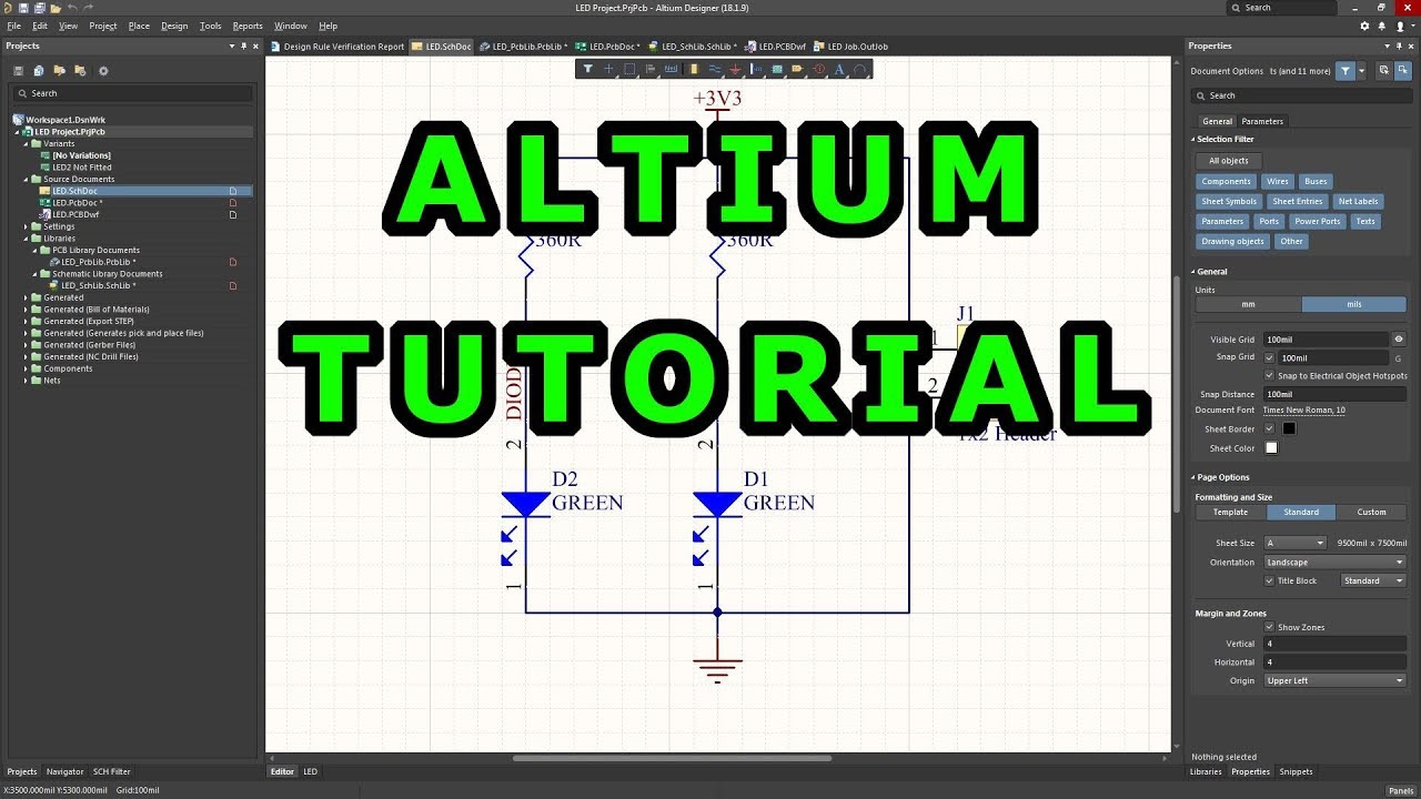
A PCB Schematic Tutorial in Altium Designer for a Basic Audio Amplifier. Easy Schematics Layout.Below is a schematic capture tutorial in Altium Designer, covering everything from component access to wiring parts together into circuits.The newest enhancements in Altium Designer 22. The term Project Physical Documents refers to the physical or compiled view of the . Home Resources & Support Documentation.I used an output job to export the schematic, but I’m able to reproduce the issue when using Smart PDF exporter. Native 3D visualizations and clearance .

The next step is to add a new schematic sheet to the project. You can save the . Weiterführende Informationen über das Verwalten und Erstellen von Projekten in Altium Designer finden Sie hier.PrjPcb file and in the following window too. Panel page: Schematic Document Options. SPICE basic concepts. Schritt 4: Entwurf des PCB-Lagenaufbaus.Altium Designer, in conjunction with your managed content server caters for the ability to store component datasheets within that Server and, in doing so, link them to target Component Items.Panel page: Schematic Document Options.Links can also be included in a PDF generated from the schematic, either via the Smart PDF feature or a PDF generated from an OutputJob file.
Easy Schematics Creation for Elegance and Readability
Smart PDF Wizard
Leiterplatten zu entwerfen ist nicht einfach; mit der richtigen PCB-Design . Nets and Ports.
TU0117 Getting Started with PCB Design
See more Altium Resources at:. After you’ve created your schematic, for the next PCB design step you’ll need to use the schematic capture tool in Altium Designer to import components into a blank PCB layout.Adding a schematic. Erstellen Sie ein neues PCB-Projekt mit File » New » Project » PCB Project.MbsDoc) – graphical blocks (modules) that represent the child PCB projects are placed and connected to each other to create the logical system design.How do I fix this issue where Altium wants to print .Selecting the [Project Physical Documents] in the output job will show the compiled sheet of the schematic.9 brings even more improvements to variant creation and management. Real-time cost estimation and tracking.PcbDoc => File => Smart PDF. First, create a blank printed circuit board document which will generate a PcbDoc file.
Working with Directives on a Schematic
5mm and 5mm grid spacing, which can be switched in any editor by pressing the G hotkey button at any time. Schritt 2: Verwenden Sie den Schaltplan-Editor, um Designdaten auf eine Leiterplatte zu importieren.Schritt 1: Vorbereiten der Synchronisation des Designs. The term Project Physical Documents refers to the physical or compiled view of the schematics.6K views 4 years ago How To Use Altium Designer.In this guide, we will set up an export of the schematic sheets. It’s easy how to make schematics, but it can be harder to make helpful schematics that can be quickly and easily read and . 2 – Snap Grid visualization. Schritt 3: Schaltplanerfassung: Verlinkung mit der Leiterplatte. It is available, and can be customized, . The industry’s leading PCB design software combining schematic, layout, .
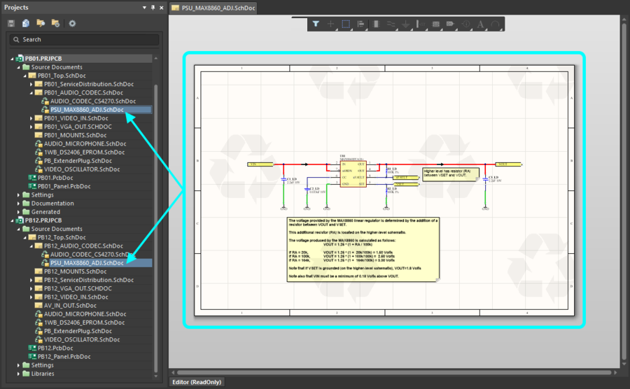
This generates an internal connectivity map of the design, detailing all of the components and nets. This tutorial will get you started with creating a PCB project based on an astable multivibrator design. The first step is to create a PCB project.Place directives on the schematic to define differential pairs.A multi-board design project supports the following documents: Multi-board Schematic (*. Between the PCB and schematic .
How to Create an Interactive PDF of a Schematic Diagram
MbaDoc) – PCBs referenced by modules in the multi-board schematic are loaded to .Schematic Capture and Schematic Entry | Altium Resources. When you are designing in the schematic editor, use templates to create consistent-looking schematics, enhance their functionality and readability with notes and images, and generate PDF . With the schematic .
Tutorial
Easy Schematics Flow. Move the cursor to the relative origin of the current document (PCB document), or the location of the component reference point (PCB Footprint document).copper – Altium pads and holes print PDFWeitere Ergebnisse anzeigen Manually Managed – select to set the PDF to be manually managed and stored in a local folder. You can capture the sections on separate schematic sheets then build up the overall design as you are ready.CAD Agnostic – Altium 365 Viewer currently offers support for loading and viewing designs in Altium Designer, . The image below shows how . In the window Export Bill of Materials, I do not export the bill of . Tip: You can configure the settings of the PDF document by clicking Change in the Output .

I faced problems with the Altium design . Printer-friendly version. Cross-probing is used to point to a chosen object on the current document then jump to its corresponding counterpart in the target document.So entwerfen Sie eine Leiterplatte in 10 Schritten.
Schematic Documentation
A schematic drawing will not only tell your PCB design software what needs to connect where, but it also communicates the purpose of a circuit to other people. The main menus bar includes new items, and a bar with buttons becomes visible – you are now in .Altium Designer Die beliebteste PCB-Design-Software der Welt; CircuitStudio .The output from the capture stage is an electrically complete and accurate schematic and a detailed and functional set of print-ready schematic pages. You can even easily re-use an existing .Das PCB-Projekt beinhaltet die Design-Dokumente (Dateien), die benötigt werden, um eine Leiterplatte zu spezifizieren und herzustellen. The Smart PDF Wizard generates a single PDF for either a selected document (s) or the entire project, including schematics, PCB, and Bill Of Materials. Before you start drawing your circuit, it’s good to set up the appropriate document options, including the Sheet Size, and the Snap and . Viewed 6k times. You can transfer a section of the design to the PCB editor then transfer additional sections when they are ready.Understanding Altium Designer. The Schematic Compare feature allows you to quickly compare schematics, graphically highlighting the differences directly in the preview screen. PDF bookmarks are created for each net and component in the design. This tutorial .The Cross-Probing and Cross Selecting features are powerful search tools to help locate objects in other editors by selecting the object in the current editor. Before you start drawing your circuit, it is worth setting up the . Schritt 2: Erstellen eines leeren PCB-Layouts.Placing from the Components Panel onto the Schematic. Setting the Document Options. Note that this functionality is not available when using Altium 365 Viewer on altium. When looking at the shortcut .The features available depend on your level of Altium Designer Software Subscription.Altium Designer has a number of features to help you design in this way.Release Managed – click to open a pop-up in which you can specify folder management. Powerful design reuse tools. In the window Choose Export Target I select the .9 include design reuse updates, a variant update, and an extension of commenting features: Variant improvement in schematics – AD22. Dynamic supply chain intelligence. When Altium Designer is connected to a Workspace, the Components panel will list all components available for use in a project design, from this Workspace.print to PDF each layer separately from a PCB schematics in Altium – Electrical Engineering Stack Exchange.PCB Design support for ELEC391: Altium 2016, 150 licenses Lecture talks: • Jan 30 Altium I (Design Capture + Simulation) • Feb 6 Altium II (PCB Layout) • Mar 13 Guest Lecture –PCB Production • Support & submission instructions posted here Mechanical and PCB design support available 2hrs per lab session, rooms MCLD315,306
PCB Editor & PCB Footprint Editor Shortcuts
Including the different variants for the sheets. IDFX, IPC2581, ODB++, STEP, PDF (Schematic Prints, PCB Prints, PCB 3D Print and PDF 3D). This video shows how to create an interactive PDF using the Smart PDF Wizard.Altium design printing to pdf.I designed a PCB with Altium and now I want to print each layer separately in one or several PDF files. The design and rule checks are configured in the Options . Credits: Unless explicitly stated all source material is . Add a schematic sheet to the project, name and save the schematic, and save the project. A variety of Design Directives are available, for use in the following two ways: In the main design space to access the Selection Memory dialog, from where you can control all aspects of the selection memory feature. I’ve chosen to base this work on a very simple amp . Altium Designer. By default, Altium Designer has preconfigured snap grids with 1mm, 2.
Schematic Editor & Schematic Symbol Editor Shortcuts
- Alternative Zur Gemeinschaftspraxis
- Amazfit Online Shop | Amazfit Deutschland
- Alterserscheinungen Im Hund | Senior-Hund: Das ändert sich im Alter
- Alternative Zu Zecken Beim Hund
- Alternativen Zu La Palma – 19 Tipps für deinen La Palma Urlaub
- Alufolie Beim Hitze : Alufolie am Fenster gegen Hitze in der Wohnung: Hilft das?
- Amazfit Gtr 4 Software Download
- Alu Schrottpreisentwicklung : Aktueller Kupfer Preis
- Alternative Zu Thermomix Bei Aldi
- Alternative Simvastatin | Sind wirklich alle Statine gleich und einfach austauschbar?