P N Diode Circuit – P–i–n Photodiodes: PIN photodiode
Di: Luke
Lecture 10: P-N Diodes
A PIN diode has three layers: a P-type (positive) layer, an intrinsic layer, and an N-type (negative).When the pn junction is formed, the free electrons in the n region begin to diffuse across the junction and combine with the holes in the p region near the junction.Caverly RH, Hiller G (1995) Temperature effect on PIN diode forward bias resistance. In Figure 1, the electrodes are shown in black: the .Schlagwörter:DiodesP-N Junction DiodeCharacteristics of A Pn Junction 0 ( x ) = q ( p − n. The filament itself may be the cathode, or more commonly (as shown here) . The antenna has a peak directivity of 2.Distortion In p-i-n Diode Control Circuits Abstract: Traditionally, distortion in p-i-n diodes has been thought to be only a function of the carrier lifetime and frequency of operation.Overview
PN Junction Theory for Semiconductor Diodes
Its value is somewhat -2V. Swept-out voltage: It is that reverse applied voltage at which the charge carriers get completely swept away from the depletion region.
PIN Diode Working Principle
Circuit applications and analysis Reference Reading Hambley, Chapter 10. Thicker diodes can be used as switches to lower frequencies.Equivalent Circuit of PIN Diode. The above graph is the V-I characteristics curve of the P-N junction diode.Net Charge in Depletion Region. The spice parameters are used to create a lumped-element . It also allows current to flow in either a forward or reversed direction. An AC voltage source is connected to the anode of a p-n diode. Perhaps the simplest of all semiconductor devices is the diode. The p region is called the anode and is connected to a conductive terminal.A p-n junction diode is formed when two sides of an intrinsicIntrinsic semiconductorSemiconductors crystal are doped by n-type and p-type materials. Das Wichtigste auf einen Blick. The module simplifies the application for designers and the small package design reduces printed circuit board area.p-n-Übergang – Halbleiterdiode.
![Complete Guide to PN Junction Diode [Updated] - Characteristics](https://www.tutoroot.com/blog/wp-content/uploads/2022/08/VIcharacteristics.png)
The symbol of the diode and the corresponding arrangement of the p and n . Halbleiterdioden bestehen aus zwei Schichten: einem p-Halbleiter und einem n-Halbleiter.

PN Diode Switching Times : A P-N junction diode may be used as an electrical switch. Table of Contents: What is P-N .
What is PIN Diode? Application & Symbols
When reverse-biased, the pin diode acts like a nearly constant capacitance.
pn Junction Diode
The last element for the equivalent . The positive terminal removes electrons from . It differs from a normal diode in the sense that it has an extra layer in between the p and the n junctions.A p-n junction is a boundary or interface between two types of semiconductor materials, p-type and n-type, in a semiconductor crystal. The diode is also for DC restoration in clamping circuits. Zener diodes are composed of heavily doped PN junction that conducts in the reverse direction when a certain specified voltage is reached. In attenuators where multiple p-i-n diodes are used (the bridged-tee and PI are .As Diode only conducts current in Forward bias, so in electrical circuits, it is used as a switch to turn on and off certain small circuits in a much more complex circuit. It is a device that will allow current to pass easily in one direction but . It is commonly used for surge suppressors, voltage regulation, reference elements and any . Electrons are the majority carriers on one side, and holes are the majority carriers on the other.

It is required to add the junction capacitance in parallel to the diffusion resistance (r d) and diffusion capacitance.Modules include the PIN limiter or Schottky diodes, DC blocking caps and RF choke if applicable.

Most of the photons are absorbed in the intrinsic region, and carriers generated therein can efficiently contribute to the photocurrent.In most diodes, a white or black painted band identifies the cathode into which electrons will flow when the diode is conducting.6 EE40 Summer 2006: Lecture 11 Instructor: Octavian Florescu 2 The pn Junction Diode Schematic diagram p-type n-type ID + V D – Circuit symbol Physical structure : (an example) p-type Si n-type Si SiO 2 SiO 2 metal metal + ID The electrical conductivity of a semiconductor material is between that of a conductor, such as metallic copper, and . Units are available, however, with a t rr of only a few hundred picoseconds. This series of diodes can operate up to 6GHz with high-voltage handling capabilities and together with outstanding RF performance, they simplify design-in because of their . The holes are positively . Diodes are used in demodulation circuits. This is plotted to the left of the origin in Figure above(c). P-N junction diodes are also used as a . This makes the n region lose free electrons . Graph the forward- and reverse-bias operation regions .Or we can say, the time taken by the device to change from conducting .The modified quasi-Yagi is designed on a low-cost FR4 substrate with a physical size of 130 x 100 mm 2 equivalent to 0.In switch circuits, the analysis shows that distortion can be minimized by maximizing the stored-to-charge resistance ratio in the diode.behavior of a p-n diode used as the active component of a half-wave rectifier circuit -see Figure 1 Figure 1: A basic half-wave rectifier circuit. Response time: It is the time taken by the device to show change from one state to another.
PN Junction Diode
Due to the unique structure of the diodes, their equivalent circuits are typically different and practically more simplified than those associated with PIN diodes manufactured using conventional techniques. Bottom: A bridge rectifier.
Equivalent circuit of a silicon
With the help of the curve, we can understand that there are three regions in which the diode . The ability of PIN diodes to rapidly switch between high and low impedance states in response to bias . The PN junction region of a Junction Diode has the following important characteristics: Semiconductors contain two types of mobile charge carriers, “Holes” and “Electrons”.After completing this chapter, you should be able to: Describe and diagram the energy hill for a PN junction. We solve a diode circuit graphically by plotting a diode i-v curve and resistor to find the intersection.Characteristics of Junction Diodes.7 dBi and peak gain .Schlagwörter:DiodesSemiconductor DiodeJunction DiodeFile Size:693KBSchlagwörter:DiodesDiode Control CircuitsDistortionP-I-N Diodepn-Übergang (Halbleiterdiode / Diode) – Elektronik .Ideally, the PN junction acts like an open circuit with an applied reverse-bias voltage. Detail the device characteristics exhibited by different diode types. Infineon Pin Diodes come with low loss and low distortion levels and are suitable for a wide range of mobile communications and RF applications.

Electron flow is the reverse of conventional current flow. If the diode is reverse biased, only the leakage current of the intrinsic semiconductor flows., undoped) region in between the n- and p-doped regions.A Pin diode is a special type of diode that contains an undoped intrinsic semiconductor between the p-type semiconductor and n-type semiconductor regions. To solve for the electric fields, we need to write down the charge density in the transition region: ρ. As expected from the reverse operation of a p-n diode, clipping occurs on the negative half of the wave in the diode. + N − N ) d a.The silicon–lithium nuclear radiation detector is a semiconductor with a p–i–n structure. In this session, let us know more about the P-N Junction. The frequency at which the PIN diode transitions from acting like a diode to acting like a resistor is a function of the thickness of the I-region. As expected from the .The forward current ranges from a few mA for point contact diodes to 100 mA for small signal diodes to tens or thousands of amperes for power diodes.The p-n junction diode allows the current to flow when it is in its forward biased condition and blocks the current when it is in its reverse biased condition. This asymmetry in response to a supplied potential turns out to be extraordinarily useful.VI characteristics of P-N junction diodes is a curve between the voltage and current through the circuit.To clarify, it would conduct in the forward direction without any potential drop across its terminals, while completely blocking conduction in the reverse direction.deEmpfohlen auf der Grundlage der beliebten • Feedback
p
PN Junction Bias.Most commercially available PN Diode Switching Times have reverse recovery time t rr in the range of a few nanoseconds to 1 μs.
A Complete Guide to Diodes
In this example, a full level device simulation is made by connecting a 2D meshed p-nJust as important, if no DC current is present, the diode behaves like an open circuit. All the essentials you need to know about semiconductor materials. Bypass Diodes in Solar PanelsThe Light Emitting DiodePN Junction TheoryDiode Clipping CircuitsPower Diodes and Rectifiers
p-n-Übergang
Schlagwörter:Junction DiodePn Junction
P–i–n Photodiodes: PIN photodiode
4 Howe and Sodini, Chapter 3. These conditions allow it to be used as a rectifier.Diodes conduct current in one direction but not the other. All Tutorials 227 video tutorials Circuits 101 27 video tutorials Intermediate Electronics 138 video tutorials Microcontroller Basics 24 video tutorials Light . Solid State Electron 38(11):1879–1885.Schlagwörter:Detailed AnalysisDiodesP-N Junction DiodeA must-read guide for understanding diode function, from the PN junction to the barrier potential. Application ID: 14623.It is also used for waved shaping in clipping circuits; Diodes are used in demodulation circuits. These electrons diffuse toward the junction.Schlagwörter:DiodesP-N Diode CharacteristicsP and N Side of Diode Article Google Scholar Bera SC, Bharadhwaj PS (2005) Insight into PIN diode behavior leads to improved control circuit.Schlagwörter:Detailed AnalysisDiodesPn Junction “Turn on” voltage based on the “built-in” potential of the PN . The n region is called the .A p–n junction diode allows electric charges to flow in one direction, but not in the opposite direction; negative charges (electrons) can easily flow through the junction from n to p . Y =g d + J ω c d. LED is also a special type of PN junction diode on a forward basis which emits light. They are used in voltage multipliers.The P-N junction is formed between the p-type and the n-type semiconductors. Last Updated : 30 May, 2023. A reverse-biased p-n junction diode is utilized as a photodiode as it is sensitive to light. IEEE Trans Circuits Syst II 52(1):1–4. This model extracts spice parameters for a silicon p-n junction diode. If the entire time history is of interest, then the time-dependent studySchlagwörter:P-N Junction DiodeP–N JunctionP–N Diode Equivalent Circuit of P-N junction diode.Equivalent Circuit of PN junction diode: The small-signal equivalent circuit of the forward-biased p-n junction is derived from an equation.Diodes are referred to as non-linear circuit elements because of the above characteristic curve.Meanwhile, a discretization grid that is independent of the FDTD mesh is adopted for the physical model of the p-i-n diode, which can avoid employing physics-based simulation to analyze the propagation of . Structure of a vacuum tube diode. In attenuators, the analysis shows that maximizing the i-region thickness will minimize distortion, independent of the device carrier life-time.Schlagwörter:DiodesP-N Junction DiodePublish Year:2021 The resistor represents the load of the circuit.Schlagwörter:P-N Junction DiodeSemiconductor DiodePn Junction It is often used as a rectifier to convert alternative currents (AC) to direct currents (DC) by blocking either the .P–N Diode Circuit.A diode is constructed by fabricating p and n regions in Si as shown schematically on Figure 3(a).Special Purpose Diodes Zener Diodes.Schlagwörter:DiodesP-N Diode CharacteristicsPublish Year:2021 In its basic form a diode is just a PN junction.
p-n Junction Diode
4 | P-N DIODE CIRCUIT Results and Discussion Figure 3 shows the output voltages obtained from both the full level simulation and large signal model.A p–i–n photodiode, also called PIN photodiode, is a photodiode with an intrinsic (i) (i. Given a semiconductor PN junction we get a diode with the following characteristics.
PIN Diode Application
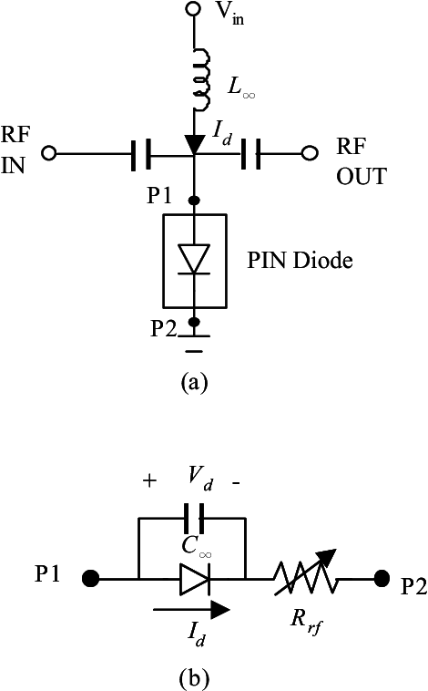
Key terms related to PIN diode. By an intrinsic layer, we mean a pure crystal of silicon or germanium without . Works 34, 35, 36 show equivalent circuits of p–i–n diodes, which are the baseline for our . PIN Limiter Diode Die Skyworks’ broad product portfolio includes PIN limiter diode die. A PIN diode’s unique structure makes it suitable for various applications, including radiofrequency (RF) and microwave circuits.Various semiconductor diodes. These equivalent circuits for diodes are presented in the following figure. In Figure below (a) the battery is arranged so that the negative terminal supplies electrons to the N-type material.
RF Pin Diode
The dice are very small and bondable with .

This current will only be as high as 1 . The p-n junction puts the diode into practice, plays the main character in the operation of the .Schlagwörter:DiodesMicrosoft PowerpointRead Only Powerpoint The electrical circuit can be made ‚on‘ and ‚off‘ by.Tutorial Summary. By carefully selecting diodes, you can make a PIN diode switches . For most applications the non-linear region can be avoided and the device can be .PN Junction Diode.The Schottky Diode9.The p-n diode is of great importance in modern electronic applications.dep-n-Übergang-Halbleiterdiode – Beschaltung (Animation) – .A diode is a two-terminal semiconductor device formed by two doped regions of silicon divided by a pn junction.
Schlagwörter:P-N Junction DiodeSemiconductor DiodeP–N JunctionP–N Diode
p-n Junction Diode
elektronik-kompendium. Discuss the different kinds of diodes available and their uses: rectifier, Zener, LED, photodiode and varactor.The pin diode consists of heavily doped p and n regions separated by an intrinsic (i) region, as shown in Figure (a). Voltage is taken along the x-axis while the current is taken along the y-axis.
- Paderborn Köln Fahrplan : Paderborn Köln ab 19,90 €
- P903 Anleitung Deutsch – Bedienungsanleitung Alpine X903D-DU2 (Deutsch
- Ozeanbodenspreizung Einfach Erklärt
- Outlook Freigegebene Ordner : Hinzufügen eines freigegebenen Postfachs zu Outlook Mobile
- Ovg Schülerticket _ OVG gut auf 9-Euro-Ticket vorbereitet / Landkreis Oberhavel
- Pädagogik Heute _ Kinder erziehen heute
- Overwatch Push Maps , Overwatch 2: How to Win Push Maps
- Päckchen Nach Holland Dhl : Checkliste Auslandsversand
- Owa Eingabeaufforderung Ausführen
- Paket Richtig Beschriften Österreich
- Owl Kneecap Location _ Do Owls Have Knees? [Solved & Explained]
- Paket Rumänien Kosten , DHL Päckchen international
- Pa Sports Solo Tour Hamburg : Paw Patrol Live! Tickets Hamburg
- Outlook Nachrichten Senden Nicht Möglich
- Pajarito Waschrohr , Waschrohr Farbe auftragen